YAMAHA CA-S1
¥ 95,000 (around 1978)
Commentary
This pre-main amplifier was developed based on the technology obtained in C-2a and B-3 with the aim of being the best amplifier.
The basic circuit configuration is as follows : DC equalizer with low-noise Dual FET at the first stage → DC flat amplifier with almost the same configuration as the equalizer → High Speed High-f with Ro control that can continuously change the output impedance of the amplifier from -1 Ω to + 1 Ω.TIt consists of a DC main amplifier with transistor, and is equipped with a low-noise MC head amplifier and a tone control with continuously variable turnover frequency.
We have introduced the HP-IB audio analyzing system, which combines a spectrum analyzer and a computer, and have examined the characteristics of each unit amplifier at a level beyond the analysis limit of conventional measuring instruments.
A new function is the Ro (output impedance) control circuit that can continuously vary the output impedance of the amplifier from + 1 Ω to -1 Ω.
This circuit is controlled by detecting the output current of the amplifier, passing it through the Ro control amplifier, and adding it to the NFB circuit of the power amplifier. This reduces the deterioration of characteristics caused by the resistance of the speaker cord or the tone control for the speaker.
The equalizer circuit consists of a differential input current mirror cascode bootstrap with a low-noise Dual FET, a Darlington connection pre-drive, and a DC amplifier with a pure CON SEPP-OCL.
The first stage low-noise dual FET combines the electrical and thermal characteristics of the two high-gm FETs in the same package. It has excellent characteristics as the first stage element of the DC amplifier configuration.
In addition, the current mirror circuit provides sufficient gain and low distortion factor, and the degradation of distortion factor is suppressed to a small value by the increase of signal source impedance at high frequency when the cartridge is connected by the cascode bootstrap circuit.
The second stage is an emitter-grounded amplifier circuit with a Darlington-connected constant voltage load, reducing the load to the first stage, and the output stage is f with well aligned pair characteristics.TIt is a pure con SEPP-OCL circuit with high transistors, and the output impedance is designed to be low enough to obtain large output voltage with low distortion factor.
In addition, the use of high-precision capacitors and resistors provides excellent RIAA deviation characteristics.
The circuit of the flat amplifier is almost the same as that of the equalizer amplifier. It has a low output impedance of 220 Ω with the configuration of the DC amplifier consisting of the first stage in which a current mirror and a cascode bootstrap circuit are assembled into a differential amplifier circuit using a low-noise FET, grounded emitter amplifier, and Pure-Con SEPP-OCL.
In addition, this flat amplifier uses a cascode bootstrap circuit in the first stage as well as the equalizer stage, so that the distortion factor is prevented from changing due to changes in the signal source impedance of other devices connected to the input of the flat amplifier.
The first stage of the main amplifier consists of a high-gm dual-FET source follower designed for low noise and a balanced feed differential amplifier circuit with cascode-connected dual transistors. The second pre-drive stage is also a current mirror push-pull differential amplifier circuit. Like the equalizer flat amplifier, this stage uses a cascode-bootstrap circuit to minimize the increase in distortion due to changes in signal source impedance.
The current mirror circuit used in the pre-drive stage provides sufficient gain as a voltage amplifier stage, and the two transistors function as a kind of push-pull circuit to cancel out the harmonic distortion of even order.
In addition, DC drift due to temperature change and time of the midpoint voltage, which is a problem especially in DC amplifier, is suppressed very little by adoption of dual FET and cascode bootstrap circuit, and high stability, high slew rate and low distortion voltage amplification stage is realized.
In addition, the power amplifying stage includes a High-Speed High-f.TIt is a 3-stage Darlington connected pure complimentary service parallel push-pull OCL circuit composed of transistors, and High-f with good matching pair characteristics.TThe 3-stage configuration of the transistor provides sufficient power gain over a wide bandwidth, rapidly discharges the accumulated charge in each stage, and improves stability at no load.
In order to bring out the performance of this output transistor, a series of diodes and resistors are connected between E-E of the drive stage to make the resistance value sufficiently low. This reduces the charge discharge impedance of the base region and makes it the main part to rise and fall.
The MC head amplifier uses a circuit configuration of four carefully selected low-noise transistors.
The tone control circuit employs a variable turn-over frequency type. The circuit configuration consists of a tone amplifier with an audio IC of input differential and output SEPP-OCL, a pseudo-variable inductor with four transistors for continuously varying the turn-over frequency, and a pseudo-variable capacitor with four transistors. This allows for continuous variable turn-over frequency and subtle control of the program source over a wide frequency range.
Because of the electrically produced inductor and capacitor, it is strong against electromagnetic induction, and combined with the tone amplifier IC, it has high SN ratio and low distortion rate characteristics. This tone control circuit is set to 0 dB gain and can be removed from the signal path by setting the Tone Circuit switch to the Bypass position.
In order to improve the S / N ratio in actual use, a high-precision four series volume is adopted. Two series volumes per one channel are inserted into the input side and output side of the flat amplifier to reduce the volume. The actual characteristics in actual use are greatly improved.
In the construction of CA-S1, nearly symmetrical layout pattern with a copper ground line centered on the main sheet to make the impedance of the ground line sufficiently low.
The ± B power supply is laid out so that it can be balanced in both vertical and horizontal directions. Negative feedback is taken out from the output side of the arrangement as much as possible to reduce output impedance. In addition, the speaker selector switch is brought to the rear panel by an extension shaft to be integrated with the speaker terminals. The connection with the main seat is shortest.
On the input side, the pin jack and amplifier section are directly connected without using a shield wire. For important parts for sound quality and characteristics, copper plate grounding is used to reduce impedance.
Carefully selected parts are used, and especially important parts for sound quality are selected by the sense of hearing. For the capacitor inserted into the output of the equalizer, a Yamaha custom coupling capacitor for audio is used. For the Chemicon, a low-impedance Chemicon is used. To compensate for the limitation of Chemicon, a Mylar capacitor is connected in parallel to suppress the impedance rise in the high-frequency range.
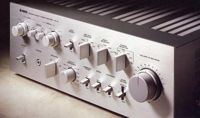
Equipped with a Phono selector, the load impedance of the cartridge can be selected from 4 levels.
It also has an MC position.
The Rec Out Selector allows you to select the rec out signal regardless of the source being played.
It is equipped with a subsonic filter, audio muting, loudness and a mono switch for switching between stereo and mono.
Built-in pre-out and main in terminals.
.JPG)
.JPG)
.JPG)
Model Rating
| Type | Pre-main amplifier | ||
| Effective output (20 Hz to 20 kHz, distortion 0.01%) | 90W + 90W (8 Ω) | ||
| Power Bandwidth (8 ω, 45W, 0.01% distortion) | 10 Hz to 50 kHz | ||
| Output impedance control | Variable impedance range : -1 Ω to + 1 Ω (20 Hz to 20 kHz) Damping factor at 0 Ω position : 100 or more (1 kHz, 8 Ω) |
||
| Input Sensitivity / Impedance | Phono1 mm : 2.5mV/100 Ω, 33k Ω, 47k Ω, 68k Ω Phono1 MC : 200 μ V/100 Ω Phono2 mm : 2.5mV/47k Ω AUX, Tuner, Tape1, 2 : 150mV/47k Ω Main in : 1V/47k Ω |
||
| Maximum Allowable Input (Distortion 0.01%) | Phono1 MM:250mV(1kHz) Phono1 MC:10mV(1kHz) Tuner : 15 v (20 Hz to 20 kHz) |
||
| Rated Output / Impedance / Maximum Output | Rec out : 150mV/600 Ω
|
||
| Frequency characteristic | Phono → Rec out : 20 Hz to 20 kHz ± 0.2 dB (RIAA deviation) Tuner → SP out : 4 Hz to 100 kHz + 0 -1dB (8 Ω) |
||
| Total harmonic distortion rate (20 Hz to 20 kHz) | Phono1, 2 mm → Rec out (5 V) : 0.003% or less (0.001% or less) Phono1 mc → Rec out (3 v) : 0.01% or less AUX, Tuner, Tape1, 2 → Pre out (3 v) : 0.003% or less (0.001% or less) AUX, Tuner, Tape1, 2 → SP out (45W) : 0.005% or less (0.004% or less) Phono1 mm → SP out (Volume-30dB, 45W) : 0.005% or less (0.004% or less) Main in → SP out (8 Ω, 45W) : 0.005% or less (0.003% or less) * The sum of harmonics up to the 10th order by HP-IB is shown in parentheses. |
||
| Intermodulation distortion factor (60 hz : 7 khz = 4 : 1) | Tuner → SP out : 0.003% or less (45W, 8 Ω) | ||
| Signal-to-noise ratio (IHF A network) | Phono1 MM:87dB Phono1 MC:73dB AUX, Tuner, Tape1, 2 (Tone on) : 102 dB AUX, Tuner, Tape1, 2 (Tone bypass) : 110 dB Main:120dB |
||
| Residual noise | 25 μ V or less (IHF A network, Volume MIN) | ||
| NDCR | Phono1 mm → SP out : 4 mW to 90 mW (1 kHz, distortion 0.01%, Volume -20dB) | ||
| Tone control characteristics | Bass : 100 Hz to 500 Hz Continuously Variable Treble : continuously variable from 1 kHz to 5 kHz |
||
| Subsonic filter | 15 Hz, 12dB/oct. | ||
| Loudness (Volume -40dB) | 100 Hz : + 10 dB, 10 kHz : + 6 dB | ||
| Channel Separation (1 kHz) | AUX, Tuner, Tape1, 2 → SP out : 65 dB (5.1k Ω short) Phono1, 2 mm → SP out : 65 dB (Input 5.1k Ω short, Volume -30dB) Phono1 mc → SP out : 65 dB (Volume -30dB) |
||
| Audio Muting | -20dB | ||
| AC outlet | Switched : two systems Unswitched-One system |
||
| Power supply voltage | 100 VAC, 50Hz/60Hz | ||
| Rated power consumption | 250W | ||
| External dimensions | Width 435x Height 162x Depth 372 mm | ||
| Weight | 14.5kg |