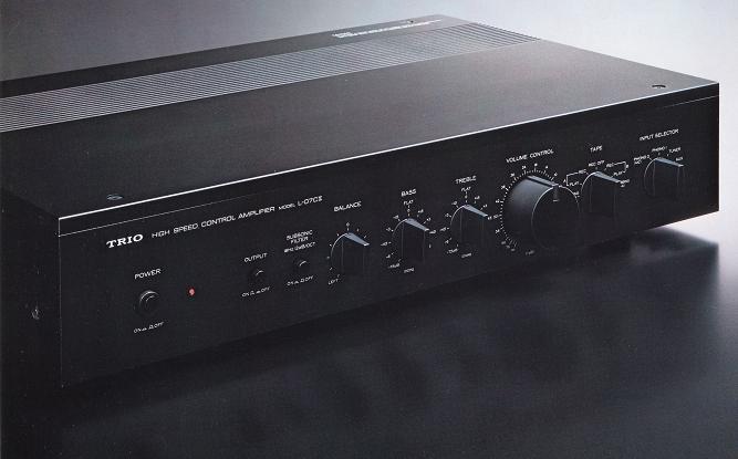
TRIO L-07CII
¥ 160,000 (around 1979)
Commentary
A control amplifier with a built-in ultra-low impedance output circuit of 10 Ω or less in order to faithfully transmit the input signal waveform to the power amplifier near the speaker system.
A buffer amplifier with an output impedance of 10 Ω or less is built in so that the audio cable can be extended to the power amplifier installed near the speakers. Thus, even if a 20-meter shielded cable of 180PF/m is connected, the frequency response drops only 0.1 dB at the ultra-high frequency band of 500 kHz, and the high-frequency loss in the cable is hardly a problem.
In addition, since the performances of this buffer amplifier are directly related to residual noise, the circuit structure has been elaborated. It is a full-scale amplifier circuit in which NFB is multiplied by 100% in the first stage cascode differential amplification and the last stage complimentary service push-pull, and noise reduction of residual noise of 3 μ V or less has been achieved.
For the equalizer amplifier, we have developed and adopted a circuit with a low distortion factor and high S / N ratio after careful consideration.
The second stage is equipped with an emitter-follower, the third stage is equipped with a current mirror, and the final stage is equipped with a pure complimentary service SEPP.
Even at low impedance, it operates with a low distortion a low distortion rate, ensuring a large dynamic range, resulting in a low distortion rate of 0.003%, which is below the measurement limit.
The SN ratio is 90 dB for an input of 2.5 mV, and the noise level is approximately 0.079 μ V and -142dBV in the input equivalent IHF A corrected value.
In addition, unlike transistors, the SN ratio of the FET used for input is not affected by the impedance of the signal source to which it is connected. Therefore, the cartridge to which the FET is connected can be selected.
In order to simplify the signal flow of the MC cartridge, the L-07CII does not insert a head amplifier before the equalizer amplifier. Instead, a full-scale MC equalizer amplifier with high gain in one NF loop is incorporated into the PHONO2 position.
As a result, the signal path of the MC cartridge can be simplified from the PHONO input to the equalizer amplifier, and the sound quality is greatly improved.
The circuit consists of two stages of FET input differential to stabilize amplification and further reduce impedance to improve SN ratio.
The input impedance is 600 Ω, which is close to the operating condition of the cartridge and does not decrease the signal level.
The tone control circuit switches between a resistor and a capacitor by means of a switch so that one step changes precisely by 1.5 dB.
Since the total variable range is limited to within ± 7.5 dB, the signal level does not vary greatly depending on the frequency and low distortion can be maintained.
When the knob is in the center flat position, all CR elements such as capacitors are disconnected from the circuit.
The buffer amplifier consists of a cascode differential circuit with a current mirror at the first stage and a complimentary service push-pull at the last stage. It is designed with low impedance, low noise and low distortion factor.
The left and right amplifier circuits are divided at the center line of the printed circuit board in order to completely eliminate various crosstalk caused by interference between the left and right circuits or their parts, or coupling of wiring and circuit loops.
At this center line and along the signal flow, we placed switches and volumes that are tightly shielded internally.
As printed circuit boards for signal circuits, we have adopted double-sided boards made of glass-epoxy material with the same performance as those used in measuring instruments that require high insulation and stability, thereby suppressing various sound quality degradation caused by changes in temperature and humidity.
The volume is uniform in thickness and has a smooth surface of less than 0.2 μ m. It uses conductive plastic, a new resistor which is extremely smooth. Although it is a variable resistor with slider, its internal noise is lower than that of ordinary PD resistance and it is a very reliable volume.
A high-performance film capacitor made of polypropylene is used for the equalizer amplifier. Film with low dielectric loss is wound with high-quality electrode foils at the optimum tension, and the electrode foils and lead wires are tightly connected to each other. Thus, the amplifier is resistant to the influence of external vibration and self-vibration and always ensures a sufficiently low distortion factor.
.JPG)
.JPG)
Model Rating
| Type | Stereo control amplifier | ||||||||||||||
| Input Sensitivity / Impedance |
|
||||||||||||||
| Signal-to-noise ratio |
|
||||||||||||||
| Output Level / Output Impedance | Tape Rec : 140mV/100 Ω Out Put : Rated output 1V/10 Ω or less |
||||||||||||||
| Rated load | 50k Ω | ||||||||||||||
| Maximum Allowable Input (1 kHz) | Phono1:450mV Phono2:40mV |
||||||||||||||
| Frequency characteristic | Tuner, AUX, Tape : 1 hz to 3.5 mhz + 0 db -3dB | ||||||||||||||
| RIAA deviation | Phono1 (MM) : 20 Hz to 20 kHz ± 0.2 dB Phono2 (MC) : 30 Hz to 20 kHz ± 0.2 dB |
||||||||||||||
| Total harmonic distortion factor |
|
||||||||||||||
| Tone control | BASS : 100 Hz ± 7.5 dB TREBLE : 10 kHz ± 7.5 dB |
||||||||||||||
| Subsonic filter | 18 Hz, 12dB/oct. | ||||||||||||||
| Channel separation | 100 dB (Aux, short circuit) | ||||||||||||||
| Transient response Rise time |
VRMAX : 0.1 μ S (+ 0.1 V to -0.1 V, + 1 V to -1V, + 2.5 V to -2.5 V) VR-6dB : 0.2 μ S (+ 0.1 V to -0.1 V, + 1 V to -1V, + 2.5 V to -2.5 V) |
||||||||||||||
| Rated power consumption | 50W (Electrical Appliance and Material Control Law) | ||||||||||||||
| Pwer | 100V 50Hz/60Hz | ||||||||||||||
| Power outlet | Power Switch Interlock : 3 pcs / 300W Power Switch Not Linked : 1 Piece / 100W |
||||||||||||||
| External dimensions | Width 480x Height 100x Depth 340 mm | ||||||||||||||
| Weight | 8.2kg | ||||||||||||||