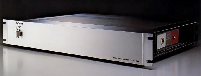
SONY TA-N88
¥ 180,000 (released in 1977)
Commentary
A high-grade stereo power amplifier equipped with a PWM system (pulse width modulation system) and PLPS (pulse lock power supply) utilizing digital technology.
The TA-N88 uses the Pulse Width Modulation (PWM) method.
In the analog amplification method used in conventional audio power amplifiers, the output side of a power amplifier is inserted between a load (speaker) and a power supply, and the power flowing to the load is extracted by changes in the internal resistance of the element. In contrast, in the PWM method, which handles pulse signals, the output can be extracted by the ON/OFF operation of the amplifier.
In an analog amplifier, the amplifying element functions as a resistance. In the PWM method, the amplifying element functions as a switch. Therefore, in principle, there is no power loss caused by the amplifying element in the analog amplifier. In reality, since the resistance value of the amplifying element is not 0, the efficiency is 80% - 90%.
In order to realize this digital amplifier, it is necessary to convert an audio signal into a digital signal. For example, when an analog signal of 20 kHz is amplified, this signal modulates a carrier of 500 kHz into a digital signal (PWM wave). The waveform width of the digital signal of 500 kHz (pulse wave) changes in proportion to the level of the analog signal.
On the circuit, the amplifying element performs ON-OFF operation at intervals of 2 μ sec (500 khz), and the ON-OFF time of the amplifying element changes according to the level of the analog signal. Therefore, the output is the product of the ON time of the amplifying element and the applied power voltage. This power-amplified digital signal is passed through a low-pass filter and returned to the original audio signal.
The PWM amplifier section of the TA-N88 consists of an input high-speed attenuator, a carrier oscillation circuit, an integrator circuit, a high-speed comparator circuit, a V-FET gate drive circuit, a V-FET switching circuit and a low-pass filter.
An input high-speed attenuator is an attenuator that uses an FET as a resistance element. It protects the amplifier by attenuating the input at a response speed of 1 μ sec or less so that the current flowing through the V-FET of the output stage does not exceed the rated current when the load is short-circuited by mistake or when an excessive input is applied to the amplifier.
In the carrier oscillator circuit, a sine wave of 500 kHz generated by a Colpitts oscillator circuit is converted into a square wave with uniform duty through a differential amplifier, and is sent as a carrier (carrier signal) through a buffer amplifier of an emitter follower for L and Rch.
Because the integrator circuit subtracts (integrates) the injected audio and carrier signals (square waves) from the output signal, the integrator circuit must have a very broadband frequency response from the audio band to the high-frequency band of the carrier (DC to several MHz).
Because the high-speed comparator circuit requires extremely fast response characteristics, it is composed of an IC, which is a 3-stage series of differential amplifiers. It operates with input voltage level differences of less than 1 square wave output (PWM wave) with a response time of less than 20 nsec (1/50,000,000 sec).
The V-FET gate drive circuit amplifies the approximately 8Vp-p output of the PWM modulated wave to a 40-Vp-p square wave voltage required to drive the gate of the V-FET used for power amplification in the final stage.
The V-FET switching circuit consists of a parallel push-pull circuit using four V-FETs per channel newly developed for high-power switching. This V-FET device enables high-power switching of up to 160 v and 10A in 50 nsec.
A low-pass filter extracts only the audio signal component from a pulse-width modulated signal. This circuit uses a low-loss LC-type filter with coils and capacitors.
A Pulse Locked Power Supply (PLPS) is used for the power supply.
The principle of operation of this power supply is as follows : First, 100 VAC is rectified directly, then this DC is converted into a 20 kHz pulse, transformed by a high-frequency transformer, and rectified again to obtain the power supply voltage of the amplifier. In addition, a constant voltage lock circuit using a chopper method is inserted to suppress voltage fluctuation caused by output fluctuation of the amplifier section by converting the fluctuation into pulse width and controlling it.
The pulse lock power supply consists of rush current suppression circuit, primary rectifying circuit and smoothing circuit, chopper type constant voltage circuit, 20 kHz power oscillator, pulse width control circuit, ferrite core transformer, secondary rectifying circuit and LC smoothing circuit.
In the primary rectifier circuit, input of 90 v to 130 v AC is bridge rectified to obtain 130 v to 168 v DC. In case of DC input, it is transmitted as it is along the polarity of the diode.
In the 20 kHz power oscillator, a self-excited bridge oscillation circuit using four high-power switching transistors is used to stably oscillate high power pulses of 20 kHz.
Ferrite core transformers are used to transmit 20 kHz pulses. Even at the high frequency of 20 kHz, they use ferrite cores with low loss, high magnetic permeability, and high saturation magnetic flux density. Therefore, they have 55 times more power transmission capacity than conventional power transformers used at 50 Hz. In addition, they have excellent regulation because the total wire length of the winding is shortened.
The secondary rectifier circuit supplies the necessary DC voltage to each amplifier stage. Since the primary side is constant voltage by pulse width control method, stable power output can be obtained.
In the pulse width control circuit, the square wave obtained by the 20 kHz power oscillator is converted into a triangular wave, and the level is compared with the reference voltage to obtain a pulse for controlling the chopper type constant voltage circuit.
In the chopper type constant voltage circuit, a constant voltage is maintained by electronically turning ON / OFF the DC obtained in the primary rectifying circuit by the pulse from the pulse width control circuit.
The pulse-locked power supply has the advantage of almost no ripple due to the pulse rectification system, high efficiency due to high frequency, and extremely stable power supply voltage due to the pulse-locked system.
The PWM amplifier and PLPS power supply handle frequencies as high as 500 kHz and 20 kHz, respectively. Therefore, these frequencies and their harmonics may interfere with each other or affect external devices.
To prevent this, the TA-N88 is equipped with a filter that traps harmonics at the AC input, speaker output, input terminal, etc. to prevent frequency leakage.
In addition, since the whole aluminum is a shield case made of aluminum die-cast, high-frequency pulses do not leak outside.
.JPG)
.JPG)
.JPG)
.JPG)
Model Rating
| Type | Stereo power amplifier |
| Circuit system | Amplifier : pulse width modulation (PWM) system, carrier 500 kHz Power supply part : pulse lock power supply |
| Effective power | 160W + 160W (20 Hz to 20 kHz, double-channel drive, 8 Ω, harmonic distortion rate 0.5%) |
| Harmonic distortion factor | 0.5% or Less (Effective Output) |
| Cross modulation distortion factor | 0.1% or Less (60 Hz : 7 kHz = 4 : 1 at Effective Output) |
| Damping factor | 20 (1 kHz, 8 Ω) |
| Residual noise | 100 μ V or Less (8 Ω, A Network) |
| Signal-to-noise ratio | 110 dB or more (closed circuit, A-network) |
| Frequency characteristic | 5 Hz ~ 40 kHz + 0. 5-1dB (8 Ω load) |
| Input Sensitivity / Impedance | 1.4 V (Effective Output) / 50k Ω |
| Output terminal | Suitable for 8 Ω to 16 Ω speakers |
| Semiconductor used | V-FET : 8 FET : 10 IC : 2 Transistor : 68 Diode : 47 Units |
| Pwer | 90 VAC ~ 130 V, 50 Hz ~ 400 Hz 110 VDC ~ 140 VDC |
| Power consumption | 135W |
| External dimensions | Width 480x Height 80x Depth 360 mm |
| Weight | 11kg |
| Attachment | Power cord |